eMMC (Embedded Multi Media Card) adopts a unified MMC standard interface, and encapsulates high-density NAND Flash and MMC Controller in a BGA chip. According to the characteristics of Flash, the product has included Flash management technology, including error detection and correction, flash average erasing and writing, bad block management, power-down protection and other technologies. Users do not need to worry about changes in the flash wafer process and process inside the product. At the same time, the eMMC single chip saves more space inside the motherboard.
Simply put, eMMC=Nand Flash+controller+standard package
The overall architecture of eMMC is shown in the following picture:
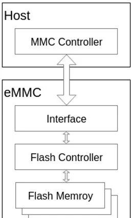
eMMC integrates a Flash Controller inside it to complete functions such as erase and write equalization, bad block management, and ECC verification, allowing the Host side to focus on upper-layer services, eliminating the need for special processing of NAND Flash.
eMMC has the following advantages:
1. Simplify the memory design of mobile phone products.
2. The update speed is fast.
3. Speed up product development.
eMMC standard
JEDD-JESD84-A441, published in June 2011: v4.5 as defined in the Embedded MultiMediaCard (e•MMC) Product Standard v4.5. JEDEC also released JESD84-B45: Embedded Multimedia Card e•MMC), an electrical standard for eMMC v4.5 (version 4.5 devices) in June 2011. In February 2015, JEDEC released version 5.1 of the eMMC standard.
Most mainstream mid-range mobile phones use eMMC5.1 flash memory with a theoretical bandwidth of 600M/s. The sequential read speed is 250M/s, and the sequential write speed is 125M/s.
The new generation of UFS
UFS: Universal Flash Storage, we can regard it as an advanced version of eMMC, which is an array storage module composed of multiple flash memory chips, master control, and cache. UFS makes up for the defect that eMMC only supports half-duplex operation (read and write must be performed separately), and can achieve full-duplex operation, so the performance can be doubled.
UFS was subdivided into UFS 2.0 and UFS 2.1 earlier, and their mandatory standards for read and write speed are HS-G2 (High speed GEAR2), and HS-G3 is optional. The two sets of standards can run in 1Lane (single-channel) or 2Lane (dual-channel) mode. How much read and write speed a mobile phone can achieve depends on the UFS flash memory standard and the number of channels, as well as the processor’s ability to use UFS flash memory. Bus interface support.
UFS 3.0 introduces the HS-G4 specification, and the single-channel bandwidth is increased to 11.6Gbps, which is twice the performance of HS-G3 (UFS 2.1). Since UFS supports dual-channel bidirectional read and write, the interface bandwidth of UFS 3.0 can reach up to 23.2Gbps, which is 2.9GB/s. In addition, UFS 3.0 supports more partitions (UFS 2.1 is 8), improves error correction performance and supports the latest NAND Flash flash media.
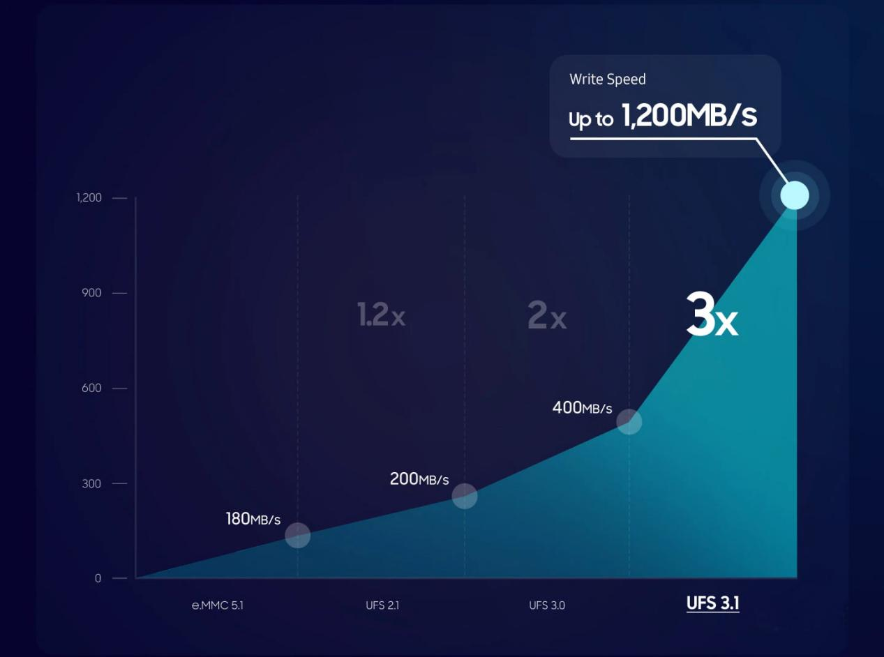
To meet the needs of 5G devices, UFS 3.1 has 3 times the write speed of the previous generation of general-purpose flash storage. The drive’s 1,200 megabytes per second (MB/s) speed enhances high performance and helps prevent buffering while downloading files, allowing you to enjoy the low-latency connectivity of 5G in a connected world.
Write speeds up to 1,200MB/s (write speeds may vary by capacity: 128 gigabytes (GB) up to 850MB/s, 256GB and 512GB up to 1,200MB/s).
UFS is also used in solid-state U disk, 2.5 SATA SSD, Msata SSD and other products, UFS replaces NAND Flash for use.
Post time: May-20-2022


