The processing process of Nand Flash
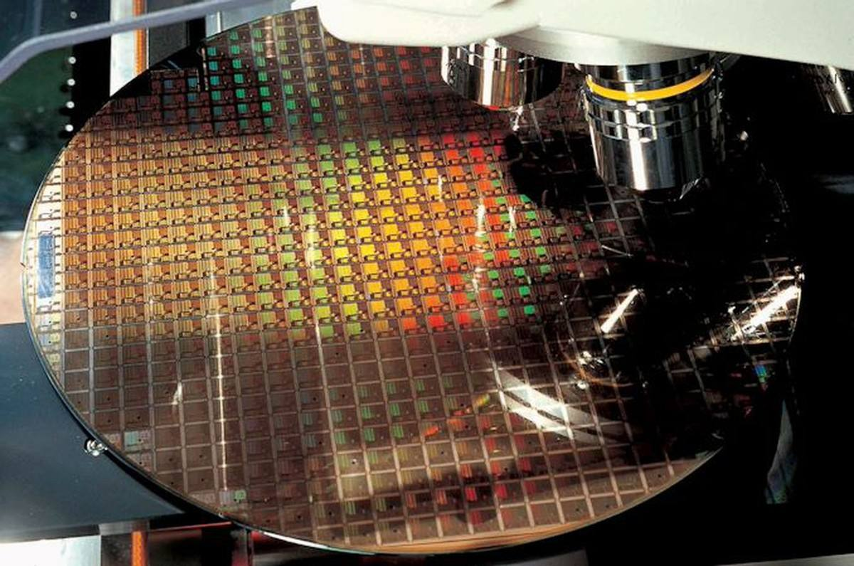
NAND Flash is processed from the original silicon material, and the silicon material is processed into wafers, which are generally divided into 6 inches, 8 inches, and 12 inches. A single wafer is produced based on this whole wafer. Yes, how many single wafer can be cut from a wafer is determined according to the size of the die, the size of the wafer and the yield rate. Usually, hundreds of NAND FLASH chips can be made on a single wafer.
A single wafer before packaging becomes a Die, which is a small piece cut from a Wafer by a laser. Each Die is an independent functional chip, which is composed of countless transistor circuits, but can be packaged as a unit in the end It becomes a flash particle chip. Mainly used in consumer electronics fields such as SSD, USB flash drive, memory card, etc.
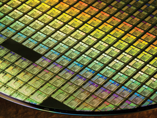
A wafer containing a NAND Flash wafer, the wafer is first tested, and after the test is passed, it is cut and re-tested after cutting, and the intact, stable, and full-capacity die is removed, and then packaged. A test will be carried out again to encapsulate the Nand Flash particles that are seen daily.
The rest on the wafer is either unstable, partially damaged and therefore insufficient capacity, or completely damaged. Taking into account the quality assurance, the original factory will declare this die dead, which is strictly defined as the disposal of all waste products.
Qualified Flash Die original packaging factory will package into eMMC, TSOP, BGA, LGA and other products according to the needs, but there are also defects in packaging, or the performance is not up to standard, these Flash particles will be filtered out again, and the products will be guaranteed through strict testing. quality.
Flash memory particle manufacturers are mainly represented by several major manufacturers such as Samsung, SK Hynix, Micron, Kioxia (formerly Toshiba), Intel, and Sandisk.
Under the current situation where foreign NAND Flash dominates the market, Chinese NAND Flash manufacturer(YMTC)has suddenly emerged to occupy a place in the market. Its 128-layer 3D NAND will send 128-layer 3D NAND samples to the storage controller in the first quarter of 2020. Manufacturers, aiming to enter film production and mass production in the third quarter, are planned to be used in various terminal products such as UFS and SSD, and will be shipped to module factories at the same time, including TLC and QLC products, to expand the customer base.
The application and development trend of NAND Flash
As a relatively practical solid-state drive storage medium, NAND Flash has some physical characteristics of its own. The lifespan of NAND Flash is not equal to the lifespan of SSD. SSDs can use various technical means to improve the lifespan of SSDs as a whole. Through different technical means, the lifespan of SSDs can be increased by 20% to 2000% compared to that of NAND Flash.
Conversely, the life of SSD is not equal to the life of NAND Flash. The life of NAND Flash is mainly characterized by the P/E cycle. SSD is composed of multiple Flash particles. Through the disk algorithm, the life of the particles can be effectively used.
Based on the principle and manufacturing process of NAND Flash, all major flash memory manufacturers are actively working on developing different methods to reduce the cost per bit of flash memory, and are actively researching to increase the number of vertical layers in 3D NAND Flash.
With the rapid development of 3D NAND technology, QLC technology continues to mature, and QLC products have begun to appear one after another. It is foreseeable that QLC will replace TLC, just as TLC replaces MLC. Moreover, with the continuous doubling of 3D NAND single-die capacity, this will also drive consumer SSDs to 4TB, enterprise-level SSDs to upgrade to 8TB, and QLC SSDs will complete the tasks left by TLC SSDs and gradually replace HDDs. affects the NAND Flash market.
The scope of research statistics includes 8 Gbit, 4Gbit, 2Gbit and other SLC NAND flash memory less than 16Gbit, and the products are used in consumer electronics, Internet of Things, automotive, industrial, communications and other related industries.
International original manufacturers lead the development of 3D NAND technology. In the NAND Flash market, six original manufacturers such as Samsung, Kioxia (Toshiba), Micron, SK Hynix, SanDisk and Intel have long monopolized more than 99% of the global market share.
In addition, international original factories continue to lead the research and development of 3D NAND technology, forming relatively thick technical barriers. However, the differences in the design scheme of each original factory will have a certain impact on its output. Samsung, SK Hynix, Kioxia, and SanDisk have successively released the latest 100+ layer 3D NAND products.
At the current stage, the development of the NAND Flash market is mainly driven by the demand for smartphones and tablets. Compared with traditional storage media such as mechanical hard drives, SD cards, solid-state drives and other storage devices using NAND Flash chips have no mechanical structure, no noise, long life, low power consumption, high reliability, small size, fast read and write speed, and operating temperature. It has a wide range and is the development direction of large-capacity storage in the future. With the advent of the era of big data, NAND Flash chips will be greatly developed in the future.
Post time: May-20-2022


