The full name of NAND Flash is Flash Memory, which belongs to a non-volatile memory device (Non-volatile Memory Device). It is based on a floating gate transistor design, and charges are latched through the floating gate. Since the floating gate is electrically isolated, so Electrons reaching the gate are trapped even after the voltage is removed. This is the rationale for flash non-volatility. Data is stored in such devices and will not be lost even if the power is turned off.
According to different nanotechnology, NAND Flash has experienced the transition from SLC to MLC, and then to TLC, and is moving towards QLC. NAND Flash is widely used in eMMC/eMCP, U disk, SSD, automobile, Internet of Things and other fields due to its large capacity and fast writing speed.
SLC (English full name (Single-Level Cell – SLC) is a single-level storage
The characteristic of SLC technology is that the oxide film between the floating gate and the source is thinner. When writing data, the stored charge can be eliminated by applying a voltage to the charge of the floating gate and then passing through the source. , that is, only two voltage changes of 0 and 1 can store 1 information unit, that is, 1 bit/cell, which is characterized by fast speed, long life and strong performance. The disadvantage is that the capacity is low and the cost is high.
MLC (English full name Multi-Level Cell – MLC) is a multi-layer storage
Intel (Intel) first successfully developed MLC in September 1997. Its function is to store two units of information into a Floating Gate (the part where the charge is stored in the flash memory cell), and then use the charge of different potentials (Level), Accurate reading and writing through the voltage control stored in the memory.
That is, 2bit/cell, each cell unit stores 2bit information, requires more complex voltage control, there are four changes of 00, 01, 10, 11, the speed is generally average, the life is average, the price is average, about 3000—10000 times of erasing and writing life.MLC works by using a large number of voltage grade, each cell stores two bits of data, and the data density is relatively large, and can store more than 4 values at a time. Therefore, the MLC architecture can have better storage density.
TLC (English full name Trinary-Level Cell) is a three-tier storage
TLC is 3bit per cell. Each cell unit stores 3bit information, which can store 1/2 more data than MLC. There are 8 kinds of voltage changes from 000 to 001, that is, 3bit/cell. There are also Flash manufacturers called 8LC. The required access time longer, so the transfer speed is slower.
The advantage of TLC is that the price is cheap, the production cost per megabyte is the lowest, and the price is cheap, but the life is short, only about 1000-3000 erasing and rewriting life, but the heavily tested TLC particles SSD can be used normally for more than 5 years.
QLC (English full name Quadruple-Level Cell) four-layer storage unit
QLC can also be called 4bit MLC, a four-layer storage unit, that is, 4bits/cell. There are 16 changes in voltage, but the capacity can be increased by 33%, that is, the writing performance and erasing life will be further reduced compared with TLC. In the specific performance test, Magnesium has done experiments. In terms of read speed, both of the SATA interfaces can reach 540MB/S. QLC performs worse in write speed, because its P/E programming time is longer than MLC and TLC, the speed is slower, and the continuous write speed is From 520MB/s to 360MB/s, the random performance dropped from 9500 IOPS to 5000 IOPS, a loss of nearly half.
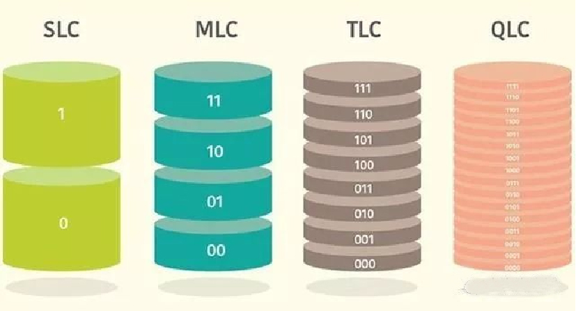
PS: The more data stored in each Cell unit, the higher the capacity per unit area, but at the same time, it leads to an increase in different voltage states, which is more difficult to control, so the stability of the NAND Flash chip becomes worse, and the service life becomes shorter, each with its own advantages and disadvantages.
| Storage Capacity Per Unit | Unit Erase/Write Life | |
| SLC | 1bit/cell | 100,000/time |
| MLC | 1bit/cell | 3,000-10,000/time |
| TLC | 1bit/cell | 1,000/time |
| QLC | 1bit/cell | 150-500/time |
(NAND Flash read and write life is for reference only)
It is not difficult to see that the performance of the four types of NAND flash memory is different. The cost per unit capacity of SLC is higher than that of other types of NAND flash memory particles, but its data retention time is longer and the reading speed is faster; QLC has larger capacity and lower cost, but due to its low reliability and longevity Shortcomings and other shortcomings still need to be further developed.
From the perspective of production cost, read and write speed and service life, the ranking of the four categories is:
SLC>MLC>TLC>QLC;
The current mainstream solutions are MLC and TLC. SLC is mainly aimed at military and enterprise applications, with high-speed writing, low error rate, and long durability. MLC is mainly aimed at consumer-grade applications, its capacity is 2 times higher than SLC, low-cost, suitable for USB flash drives, mobile phones, digital cameras and other memory cards, and is also widely used in consumer-grade SSD today.
NAND flash memory can be divided into two categories: 2D structure and 3D structure according to different spatial structures. Floating gate transistors are mainly used for 2D FLASH, while 3D flash mainly uses CT transistors and floating gate. Is a semiconductor, CT is an insulator, the two are different in nature and principle. The difference is:
2D structure NAND Flash
The 2D structure of the memory cells is only arranged in the XY plane of the chip, so the only way to achieve higher density in the same wafer using 2D flash technology is to shrink the process node.
The downside is that errors in NAND flash are more frequent for smaller nodes; in addition, there is a limit to the smallest process node that can be used, and the storage density is not high.
3D structure NAND Flash
To increase storage density, manufacturers have developed 3D NAND or V-NAND (vertical NAND) technology, which stacks memory cells in the Z-plane on the same wafer.
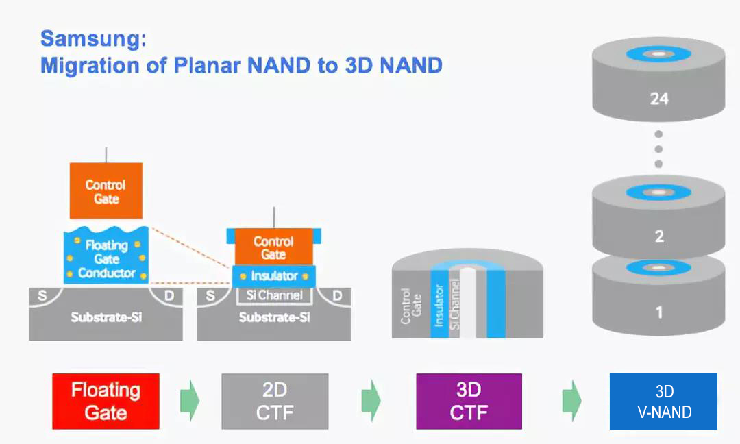
In 3D NAND flash, the memory cells are connected as vertical strings rather than horizontal strings in 2D NAND, and building in this way helps achieve high bit density for the same chip area. The first 3D Flash products had 24 layers.

Post time: May-20-2022


